Cost Considerations for RF Circuit Board
Considerations for RF Circuit Board
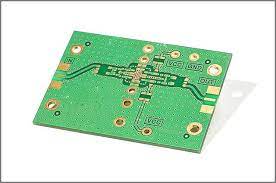
A rf circuit board is a specialized printed circuit board that operates at a high frequency to ensure the quality of transmitted and received signals. To ensure signal integrity, manufacturers optimize a PCB’s materials, layout, and fabrication processes to minimize sources of noise and interference. This includes ensuring proper shielding, sizing and positioning traces to avoid skin and coupling effects, and utilizing materials that are stable at high temperatures. In addition, RF boards must be designed to accommodate the physical constraints of wireless devices and limit transmission losses.
The cost of a rf circuit board depends on several factors, including size and design. Increasing the size of a PCB will require more materials, which can increase production costs. This is particularly true if the design requires multiple layers. The cost of a PCB also increases as the number of components increases. These components may be placed manually or using automated assembly techniques. In both cases, the cost of materials and the amount of labor required to place and solder these components can have a direct impact on the overall price of the finished product.
Unlike low-frequency PCBs, RF boards must be fabricated with materials that can withstand high frequencies and have the appropriate dielectric properties. Typical materials include FR4, Rogers materials, and Teflon substrates. These materials are often selected for their ability to withstand the high-temperature variations encountered during manufacturing. RF boards must also be carefully designed to account for the dynamic behavior of high-frequency circuits. For example, signal reflections and cross-talk between closely spaced traces can degrade performance and lead to signal loss. This can be overcome by careful alignment and stackup design.
Cost Considerations for RF Circuit Board
The manufacturing process of a rf circuit board involves complex steps that must be done with extreme precision. This is particularly important for multilayer RF boards, where the layer alignment and etching are critical to signal routing and impedance matching. Failure to maintain precise registration alignment can lead to errors in the placement and positioning of traces, which can then affect the final performance of the board. RF PCBs also require precise control of the etching process to ensure that the widths and spacing of traces match the desired specifications.
Other key factors in the cost of a rf circuit board are the thickness of the copper foil and the prepreg used to fill gaps between the copper layer. Thicker copper and the use of more prepreg are more expensive than thinner foils and less prepreg. In addition, if the manufacturing process requires specialized equipment or tools, these will add to the total cost of production.
RF circuit boards must undergo extensive testing to confirm that they meet the requirements of their intended application. This testing can include network analysis to measure S-parameters, time-domain reflectometry to assess impedance uniformity, and electromagnetic compatibility (EMC) tests. These tests help to identify sources of noise, signal degradation, and other potential problems. They can also help determine if a PCB is sufficiently shielded against external interference.